With the decline in the cost of LED chips and the advancement of technology, coupled with the recent weak growth of the LED lighting industry, domestic and foreign LED chips and packaging giants have begun to look for new market growth points, Mini & Micro LED as a new market prospects, nearly two In particular, Micro LED is currently difficult to commercialize on a large scale in a short period of time because of the uncertain technical route and high cost. MiniLED, as an extension of small-pitch LED products and a prelude to Micro LED, has begun to be in LCD backlight. And the RGB display products began to ship. At this stage, the P0.9 Mini LEDs that have been mass-produced and shipped have been used to support the small-pitch LED display because the chips, equipment and processes used are guaranteed, thus ensuring the high cost performance and quantity of the products. Production feasibility.
Mini LED backlight products are mainly concentrated in the display below 100 inches, applications include TV, e-sports, automotive, the main competitor is OLED; display products are related to 100-inch display, application areas in commercial display, large TV The competitors are small pitch display, projection, DLP, LCD splicing, etc.
Although the backlights and display products of Mini LEDs have been shipped in small quantities, the products are mainly concentrated in P0.9-0.7. The products below P0.7 are still in the stage of technology development. In the process of continuously reducing the pitch, Mini LEDs Faced with many problems such as chip, package, driver IC, backplane, etc., the following is the GGII combing the current difficulties of Mini LED technology:
1, chip end
a chip is miniaturized, because the Mini LED requires the pixel pitch to be less than 1mm, which also requires the Mini LED chip to be smaller. At present, the Mini LED chip generally requires 200um or less, which is used for lithography in the production process of the LED chip. Etching puts forward higher requirements. Especially the existing mature production equipment is difficult to meet the chip production below 100um. In the case of small size chips, the flatness of the soldering surface, the design of the electrode structure, the solderability and the adaptation to the welding parameters. Sexuality and package latitude are the difficulties and priorities of chip design. In the production process, the Mini LED chip also adopts the full-measurement full-division mode with low operating efficiency. For the processing of high-density, high-precision large-scale chips, both production and detection have inefficiencies, which inevitably pushes up. The cost of the Mini LED chip;
b. Red-light flip chip, because flip chip does not need to be wired, it is suitable for the mini-small space of Mini LED. Therefore, the current Mini LEDs all adopt flip-chip structure. At present, the production of blue-green flip-chip LED chips is relatively mature. However, the technology of red-light flipping LED chips is difficult, and the substrate transfer is required, and the yield and reliability of the chips in the transfer technology process are not high.
c. Consistency and reliability, the Mini LED chip as a display chip has higher requirements on product consistency and reliability. The indicators of consistency focus include small current consistency, uniformity under no current, high and low level consistency, color. Uniform consistency, small capacitance and consistency, etc., due to the complicated use environment of the Mini LED display, the maintenance is difficult, which requires high reliability of the Mini LED chip. In general, the Mini LED chip manufacturer is producing. Strict production control in the process to ensure the stability of various indicators of the product;
2, the package end
a, high efficiency solid crystal and patch, because the chip size of Mini LED is mainly 50-200um, while the Mini LED chip and lamp bead unit area is huge and arranged very tightly, which puts higher flatness and precision of welding surface. Requirements, adaptability to soldering parameters and package tolerance requirements are also more stringent. Therefore, the high-efficiency and high-precision Mini LED chip solid crystal becomes a problem in the face of the Mini LED. The traditional solder paste solid crystal is easy to cause the soldering drift of the chip, and the hole ratio is increased, which cannot meet the high precision solidification requirement of the Mini LED. The higher precision solid crystal substrate and the solid crystal equipment become an urgent problem to be solved. When the conventional placement machine is splicing the Mini LED package device below P1.0, since the accuracy requirement is below 25um, the conventional placement machine must reduce the placement speed to 30-50% of the original placement speed. Will greatly reduce the production efficiency of the display, more efficient placement machine is also a major problem facing the future Mini LED;
b. Thin package, when the Mini LED is used as the backlight, the thinner the product is, the better, but when the PCB thickness is less than 0.4mm, in the reflow soldering and Molding process, the chip will be induced due to the difference between the resin substrate and the copper layer thermal expansion system. In the case of Molding packaging, the difference in thermal expansion coefficient between the encapsulant and the PCB can also cause cracking;
c, mixed light consistency, due to the difference in color or circuit of the chip or lamp bead, may cause differences in display or backlight effect, which will have an adverse effect on the display effect of the Mini LED;
d, reliability and yield, the environment of the Mini LED display is relatively complicated. If the water vapor in the air penetrates into the electrode of the LED chip through the packaging material or the bracket, it is easy to cause a short circuit, and at the same time, due to the Mini LED product. A large number of densely arranged, the use of packaged devices has multiplied, considering the difficulty and cost of Mini LED maintenance, which requires the relatively high reliability of the Mini LED package.
3. Driver IC
a, current control and heat dissipation, because the Mini LED point spacing is getting smaller and smaller, the number of LED chips used is also more and more chip size is getting smaller and smaller, which leads to the drive current is getting smaller and smaller, making the drive IC current Accurate control is also becoming more and more difficult. In the future, precise control for small currents also requires new circuit design. In addition, because of the use of a large number of driver ICs and LED chips, it is difficult to quickly dissipate the PCB, and the heat will drive the IC module. The problem of color cast is generated, so the highly integrated and low power driver IC will be the development direction of the display driver IC.
b. Area dimming. For the backlight application of Mini LED, the current static dimming technology requires a high number of ICs in series, a high cost of the driving circuit, a large number of IC control I/Os, a large driving circuit, and a low backlight refreshing frequency. It is easy to have flickering, so it is difficult to meet the needs of the new Mini LED backlight technology. The regional dimming driver IC can make up for the shortcomings of static dimming, but when using the regional dimming scheme, it also faces the brightness of the Mini LED backlight partition and A series of problems such as improvement in uniformity, improvement in refresh frequency, improvement in backlight efficiency, high integration, and fine dimming resolution.
4, PCB backplane
Under the premise of slim and light Mini LED, the high requirements of display and backlight effects pose new challenges to the processing accuracy of thickness uniformity, flatness and alignment of PCB backplane, plus a large number of PCB backplanes. LED chip and driver IC, which requires the Tg point of the backplane to be higher than 220 °C, and the PCB backplane needs various external forces during the processing of the Mini LED, in order to maintain the thickness uniformity and dimensional stability of the backplane. The back plate also needs to have high physical properties such as tear strength, moisture resistance and heat resistance.
In order to expand the application of Mini LED, the upstream and downstream manufacturers of Mini LED industry are actively working on developing new technologies and reducing costs. At present, new technologies developed by Mini LED manufacturers at home and abroad focus on light-adjusting chips, COB and IMD packages, and Mini LEDs. Mass transfer, TFT circuit backplane, flexible substrate, etc.
1, light adjustment chip
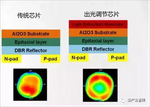
When the Mini LED is used as a backlight, a large number of LED chips are often used as a direct-type backlight. In order to adjust the light output of the chip, it is easier to realize ultra-thin design, and Huacan Optoelectronics adds an optimized film layer on the conventional backlight chip. The light-emitting angle of the chip can be improved, thereby making the light output of the LED chip more uniform and effectively improving the display effect.
2, COB and IMD package
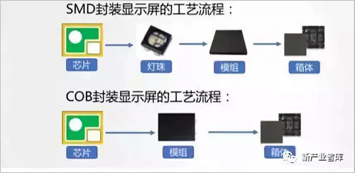
At present, the COB (on-board chip) package directly encapsulates the LED bare chip on the module substrate, and then performs integral molding, compared to the conventional SMD package. The full-color LED module of the COB package has the characteristics of less manufacturing process flow, lower packaging cost, high package integration, good display reliability and uniform display effect, and is expected to become a high-density LED display module in the future. An important form of packaging. At present, due to the fact that the COB industry chain has not yet been established, the cost per unit area of ​​COB products is higher than that of SMD. In the future, as the COB display packaging industry chain matures, the market share of COB display packaging will increase rapidly. In the Mini LED application, the COB package has higher reliability and stability, and it is easier to achieve ultra-small pitch display, which is consistent with the trend of the Mini LED technology. Therefore, the COB package is also one of the technical trends of the Mini LED.
The MiniLED for display, which was released by Guoxing Optoelectronics in June, uses Integrated Mounted Devices (IMD), a four-in-one array package, with small cells composed of two lamp beads in the horizontal and vertical directions, each of which The lamp beads are still packaged in RGB tri-color chips, breaking through the traditional design thinking and bringing together the advantages of SMD and COB, which will be a prelude to the COB package.
3, Mini LED transfer
Compared with the huge transfer technology of Micro LED, the chip size of Mini LED is relatively large, so the transfer difficulty is relatively small. Combined with the huge transfer and COB packaging technology, the production cycle of MiniLED can be effectively improved. At present, Uniqarta's laser transfer technology can Transfer by a single laser beam or multiple laser beams to transfer about 14 million 130x160 micron LED chips per hour.
4, TFT backplane
If you want to compete with OLED in the reality of the picture, Mini LED backlight + LCD must be HDR-level HDR, that is, LocalDimming Zones must have hundreds or even thousands of zones. Sufficient, but if you use a traditional LED backlight to drive the circuit architecture, the idea is that the components are used too much, at the expense of cost and thin design. In view of this, Innolux proposes an AM MiniLED architecture driven by an active matrix TFT circuit.
5, flexible substrate
The Mini LED backlight is generally designed with a direct-descent design, and a large number of dense cloths are used to achieve regional dimming in a smaller range. Since the design can be combined with a flexible substrate, the curved surface of the LCD can also be realized while ensuring image quality. Surface display similar to OLED, but due to the large number of MiniLEDs, the heat generated is huge, and the heat resistance of flexible substrates is often poor. Therefore, the development of flexible substrates with high heat resistance will be one of the future technological trends.
It is a fully automatic continuous double-station cylinder head (cylinder) cleaning equipment, with advanced structure, high production efficiency, clean and so on.The cleaning machine includes upper and lower workpiece mechanism, workstation conveying mechanism, cleaning mechanism, blowing and drying mechanism, sewage treatment device, self-lubricating mechanism, water mist collection mechanism, liquid level alarm device, etc.
Cylinder Head Cleaning Machine
Cylinder Head Cleaning Machine,Cylinder Head Cleaning Equipment,Cylinder Cleaning Machine,Cylinder Casting Cleaning Equipment
Shandong ShengKaiYuan Intelligent Technology Co.Ltd , https://www.cncastmachine.com